Home » Applications » Electronic
Electronics Industry Metal Detection & Inspection Solutions
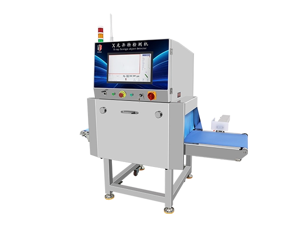
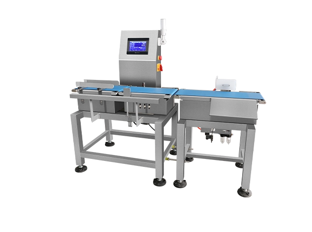
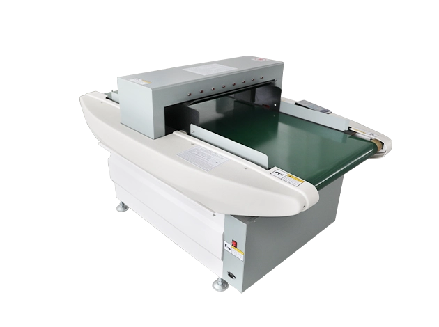
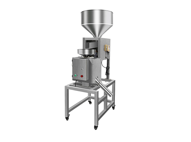
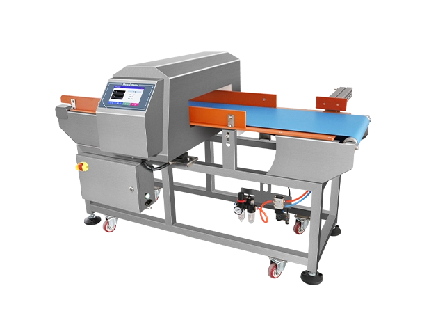
JINDUN X-Ray Inspection Equipment and Metal Separator Systems provide high-precision detection of metallic contaminants and hidden defects in electronic components, circuit boards, and semiconductor materials. Engineered for ESD-safe environments, these systems protect delicate production lines and ensure compliance with international quality standards such as IPC and ISO9001.
Our equipment integrates seamlessly with SMT assembly lines, PCB manufacturing processes, and component packaging systems, offering real-time monitoring and automatic reject mechanisms without interrupting high-speed operations. Advanced imaging and PLC control deliver reliable 24/7 performance while minimizing false alarms and maintenance downtime.
Trusted by electronics manufacturers, contract assemblers, and semiconductor facilities worldwide, JINDUN inspection solutions safeguard product integrity, reduce costly rework, and help meet the stringent reliability requirements of modern electronic devices.
Application Video
FAQS
What types of electronic products can JINDUN metal detectors inspect?
JINDUN X-Ray Inspection Equipment and Metal Separators can detect metallic contaminants or structural defects in PCB assemblies, semiconductors, IC packages, connectors, and finished electronic devices, ensuring they meet strict quality standards.
How do JINDUN systems protect sensitive electronic components from static electricity?
Our equipment is built with ESD-safe materials and grounding measures, preventing electrostatic discharge that could damage delicate circuit boards and microchips during inspection.
Can these inspection systems integrate with SMT or PCB production lines?
Yes. JINDUN X-Ray and Metal Separator units are designed for seamless in-line integration with SMT assembly and PCB fabrication lines, supporting high-speed conveyors without interrupting production.
What is the detection accuracy for tiny metallic contaminants?
Depending on product size and density, our advanced sensors and imaging technology can identify ferrous and non-ferrous particles as small as 0.2 mm, providing industry-leading precision for electronic components.
How does the automatic reject system work in electronics manufacturing?
When a contaminant or defect is detected, the PLC-controlled reject mechanism quickly diverts the affected board or component to a separate bin, ensuring only fully compliant electronics proceed downstream.


